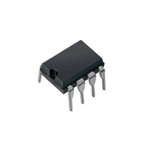
Pin Configuration
| Pin No. |
Pin Name |
Description |
| 1. |
Offset Null 1 |
Pin used for remove the offset voltage and balance input voltage. |
| 2. |
Inverting Input |
Inverting signal Input |
| 3. |
Non-inverting Input |
Non-inverting signal Input |
| 4. |
VEE |
Negative Supply Input (Ground) |
| 5. |
Offset Null 2 |
Pin used for remove the offset voltage and balance input voltage. |
| 6. |
Output |
Output of op amp |
| 7. |
VCC |
Positive Supply Input |
| 8. |
N.C. |
Not Connected |
Features
- Low power consumption
- Output short-circuit protection
- High slew rate 16 V/us
- Low input-bias and offset current
- Latch up free operation
- Internal Frequency compensation
Technical Specifications
- Voltage Supply: ±18V
- Input Supply range: ±15V
- Differential Input Voltage: ±30V
- Input Offset Voltage: 5mV
- Junction Temperature: 115℃
- (Soldering) Lead Temperature: 260℃
- Power Dissipation: 670mW
LF351 Op-Amp IC Datasheet


There are no reviews yet.