-
×
 UA741CN
1 × EGP10.00
UA741CN
1 × EGP10.00 -
×
TIP42C "PNP"power transistor"
1 × EGP10.00
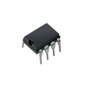 UA741CN
 Subtotal: EGP20.00

| Pin No. | Pin Name | Description |
| 1. | Offset Null 1 | Pin used for remove the offset voltage and balance input voltage. |
| 2. | Inverting Input | Inverting signal Input |
| 3. | Non-inverting Input | Non-inverting signal Input |
| 4. | VEE | Negative Supply Input (Ground) |
| 5. | Offset Null 2 | Pin used for remove the offset voltage and balance input voltage. |
| 6. | Output | Output of op amp |
| 7. | VCC | Positive Supply Input |
| 8. | N.C. | Not Connected |

There are no reviews yet.