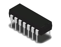
SG3525 Regulating Pulse Width Modulators
Out of stock
EGP45.00
Out of stock
SG3525 is a pulse width modulator IC. This IC is used to design all types of SMPS (Switched Mode Power Supply) and PWM signals for power electronics projects. It has improved performance and lower external parts and is a 16 pin IC. To control the output voltage, it offers a feedback circuit that controls voltage by comparing the feedback signal with a reference signal. Based on the feedback current limit, it has a protection circuit that shutdown the PWM signal. Also, this device has a built-in soft start circuit.
Generally, this device is used in inverter applications. It utilizes two main PWM outputs that are inverse of each other. A single resistor is connected between the discharge pin and CT that is used to program a wide range of deadtime. This IC has two outputs that operate in a totem pole configuration or flip flop or push-pull manner. The outputs of this IC are connected with external devices that are used to control the converter transformer for implementing final operations like MOSFET.
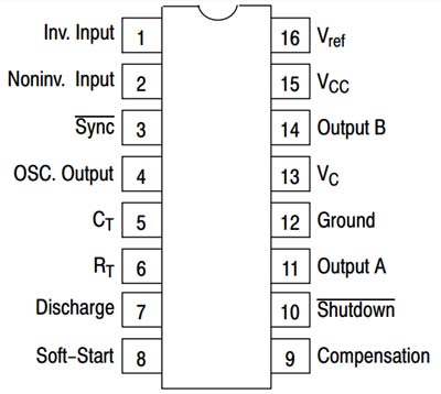
SG3525 Pinout Configuration
|
Pin Number |
Pin Name |
Pin Function |
|
1 |
INV |
Inverting Input |
|
2 |
NINV |
Non-Inverting Input |
|
3 |
SYNC |
Synchronizing IC with an external oscillator frequency. |
|
4 |
OSC. Output |
Oscillator Output. The frequency of IC is confirmed at this pin. |
|
5, 6 |
CT & RT |
These pins are used to connect an external capacitor and resistor respectively to set up the frequency of the oscillator circuit. |
|
7 |
Discharge (DIS) |
This pin is used to determine the dead time for IC. A resistor is connected between pin-7 and 5 will decide the frequency of PWM (or dead time). |
|
8 |
Soft Start (SS) |
A capacitor is connected with this pin and ground. As the name suggests, this pin is used to initiate operation softly. |
|
9 |
Compensation (COMP) |
This is a compensation pin. It is used to compensate for the error and avoid rapid fluctuations. |
|
10 |
Shutdown |
This is a shutdown pin. It instantly narrows down to PWM signals to the maximum level if it is set high. This pin is used to shutting down the output of IC in the event of malfunction or unwanted condition. |
|
11 |
Output A |
This is an output pin that is used as an input for external devices. |
|
12 |
VSS |
This pin is a ground pin. |
|
13 |
VC |
This is a power pin used to supply input voltage 5-35 V. A resister is connected to the DC supply. Therefore, this register decides the magnitude of the trigger current to the output current. |
|
14 |
Output B |
This is an output pin that is used as an input for external devices. |
|
15 |
Vin |
It is a supply input voltage 8-35 V. |
|
16 |
Vref |
It is a reference pin used to set reference voltage through pins 1 and 2. |
Features & Specifications
- Supply Voltage: 8V to 35V
- Oscillation Range: 100 Hz to 400 kHz
- Maximum Power Dissipation: 1000 mW
- 5.1 V Reference Trimmed TO ± 1 %
- Supply Voltage VCC: +40 Vdc
- Logic input: -0.3 to 5.5 V
- Output current IO: ±500 mA
- Reference output current Iref: 50 mA
- Oscillator charging current: 5 mA
- Power Dissipation PD: 1000 mW
- Thermal resistance, junction-to-Air RθJA: 100 ˚C/W
- Thermal resistance, junction-to-Case RθJC: 60 ˚C/W
- Operating junction temperature TJ: 150 ˚C
- Dual-source/sink output drivers
- Internal Soft-Start
- Pulse by pulse Shutdown
- Adjustable dead time control
- Separate oscillator sync terminal
- Latching PWM to prevent multiple pulses