 NodeMCU v2 ESP8266 Wifi Module ESP-12E Development Kit (With CP2102 Chip)
 Subtotal: EGP260.00

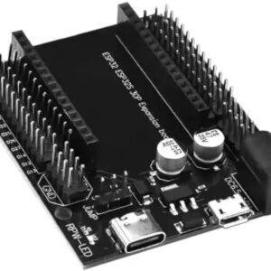
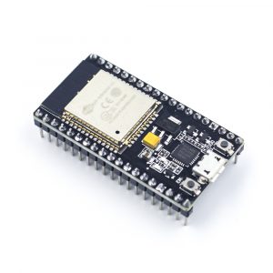
ESP32-S3 DevKitC-1 N8R2 – Dual USB-C Wi-Fi + BLE Development Board
Introduction
The ESP32-S3 DevKitC-1 N8R2 pairs the ESP32-S3 dual-core LX7 MCU with 8 MB QSPI Flash + 2 MB QSPI PSRAM, giving you enough headroom for advanced Wi-Fi/BLE projects, UI work, and ML/DSP sketches. The board exposes two independent USB functions—a classic USB-to-UART bridge and the SoC’s native USB 2.0 FS (USB-Serial-JTAG/OTG)—so you can power, flash, debug, and even make USB devices with a single cable. Most GPIOs are broken out on breadboard-friendly headers, with Boot/Reset buttons and a built-in RGB LED (GPIO48) for status.
What’s Included
-
ESP32-S3-DevKitC-1 board populated with ESP32-S3-WROOM-1-N8R2 module × 1 (8 MB Flash + 2 MB PSRAM)
Key Features
-
Dual-core LX7 up to 240 MHz: optimized for DSP/AI kernels with vector instructions.
-
Wireless combo: Wi-Fi 2.4 GHz (802.11 b/g/n) + Bluetooth 5 LE.
-
Two USB paths on board: USB-to-UART for serial/flashing and native USB 2.0 FS / USB-Serial-JTAG for flashing, debug, and USB device/host projects.
-
Memory for real apps: 8 MB Flash + 2 MB PSRAM (N8R2 variant).
-
Breadboard-friendly headers: most module GPIOs are broken out for quick prototyping.
-
On-board conveniences: Boot + Reset buttons, RGB LED on GPIO48, 5 V→3.3 V LDO regulator.
Specifications
| Parameter | Value / Notes |
|---|---|
| MCU / Module | ESP32-S3-WROOM-1-N8R2 (dual-core LX7 up to 240 MHz) |
| Wireless | 2.4 GHz Wi-Fi (b/g/n), Bluetooth 5 LE |
| Memory | 8 MB QSPI Flash + 2 MB QSPI PSRAM (module) |
| USB | USB-to-UART + native USB 2.0 FS / USB-Serial-JTAG (OTG) on board |
| I/O | Up to 36 GPIOs on the module; most available on headers +1 |
| Indicators/Controls | RGB LED (GPIO48), Boot, Reset |
| Power | Via either USB port, 5 V pin, or 3V3 pin (exclusive) |
Compatibility & Tips
-
Two ways to flash: use the UART port (legacy method) or the native USB-Serial-JTAG port for faster, driver-light flashing and JTAG debug.
-
If you use native USB in your firmware, you can enumerate as CDC, HID, MSC, etc. (USB 2.0 FS).
-
Some SPI-flash/PSRAM pins are internally used by the module—plan your GPIO map accordingly.
Use Cases
-
Wi-Fi + BLE gateways, HID gadgets over native USB, display/audio nodes, sensor hubs, TinyML/DSP demos, and beginner-friendly coursework labs.
Safety & Handling
-
Power from one source at a time (USB or 5 V pin or 3V3 pin). Avoid back-powering.
-
Observe ESD care; do not exceed absolute maximum ratings on GPIOs.
Media & Downloads
-
ESP32-S3-DevKitC-1 User Guide (v1.1) – official getting started + hardware reference.
-
ESP32-S3-WROOM-1 / 1U Datasheet – module specs, GPIOs, RF, and ordering codes (incl. N8R2).
FAQ
Q1: What exactly does N8R2 mean?
A: N8 = 8 MB QSPI Flash; R2 = 2 MB QSPI PSRAM in the module variant.
Q2: Can I power and program from either USB port?
A: Yes. Both ports can power the board; use UART for classic flashing or native USB-Serial-JTAG for flashing/debug and USB device features.
Q3: Does the board break out most GPIOs?
A: Yes—most module pins are on headers; SPI flash/PSRAM pins remain dedicated.